Datapath

Let’s recap much of what we’ve seen so far:
We’ve seen that everything—every value, every signal, every string—is composed of two values: 1 and 0.
We’ve seen how signed and unsigned integers are represented by the computer, and that the exact same bitstring can be interpreted as different values. As an 8-bit unsigned integer, the bitstring 1011 0111 has the value 183. Interpreted as an 8-bit signed integer under two’s complement, this has the value -73. Other types are no different: they consist only of zeros and ones. Data, including numeric data, strings, and other types are zeros and ones. Instructions are just zeros and ones. It’s just a matter of how these zeros and ones are interpreted and what’s done with them that matters.
We’ve learned about logic gates and how we can construct useful circuits out of them, including combinational circuits such as:
- multiplexers,
- encoders and decoders,
- half adders, and
- full adders,
and sequential circuits, such as:
- SR and D latches,
- D flip-flops,
- registers,
- etc.
We’ve seen how to construct a ripple-carry adder out of full adders, chained together, and ripple-carry adders that support subtraction with the addition of multiplexers and inverters.
All of the aforementioned circuits are constructed from logic gates and their language is binary. These are the building blocks of digital logic: gates, combinational circuits such as multiplexers, decoders, and adders, and sequential circuits such as latches, flip-flops, and registers.
Now we will take a look at a bigger picture: the datapath.
The datapath
The datapath consists of the CPU’s control unit, an arithmetic logic unit (or units), multipliers, registers, flags, and a bus (or buses) that connects them. The datapath is responsible for executing arithmetic operations, moving or copying data, and performing comparisons.
Let’s start by situating the relevant components in an appropriate context. Here’s a block diagram showing key components in a CPU (idealized and simplified).
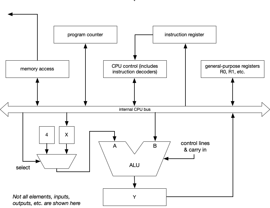
This diagram shows the CPU control (which includes instruction decoders), special purpose registers such as the instruction register and program counter, general purpose registers, and an arithmetic logic unit (ALU). The ALU consists of an adder like we’ve seen, with additional circuitry for setting flags, the status (or flag) register, increment / decrement circuits, and multiplication / division support. It also includes a logic unit which performs bitwise operations, comparisons, and bit-shifting operations. A multiplexer is used to select the current operation. All of this is contained within the ALU.
The datapath is the collection of hardware components in a processor that does the work of computation: taking operands from registers, performing computations, and writing back to memory.
It includes the major building blocks that transform and route data:
- registers for temporary storage of operands and results,
- an ALU (arithmetic logic unit) for performing computations,
- multiplexers (MUXs) to select data paths based on control signals,
- a program counter (PC) to hold the address of the next instruction, and
- memory access units for reading/writing instructions and data to memory.
Each of these components plays a specific role in the fetch–decode–execute cycle.
Revisiting fetch-decode-execute
Let’s revisit the execution cycle, now in context of hardware:
- Fetch:
- Use the program Counter (PC) to get the next instruction address.
- Fetch the instruction from memory.
- Load the instruction into the instruction register.
- Increment and update the program counter.
- Decode:
- Use control unit logic to divide the instruction into individual fields (e.g., operation class, opcode, operands).
- Determine which operation to perform (e.g., ADD, SUB, LOAD).
- Generate control signals to guide the datapath.
- Execute:
- Route operands from registers to the ALU (often via multiplexers (MUXs).
- Compute some result in ALU.
- Write the result back into a register or memory.
Key datapath components
Registers
Registers are small, fast memory units inside the CPU that hold:
- inputs to the ALU,
- results of operations,
- intermediate data, and
- special values like return addresses or constants.
Each register is built from multiple flip-flops and is updated only on the clock edge. Registers, along with appropriate decoders, are assembled into a register file. A register file has ports for
- register selection codes,
- a value to write,
- output of values read from registers.
It also has a control line used to enable writing.
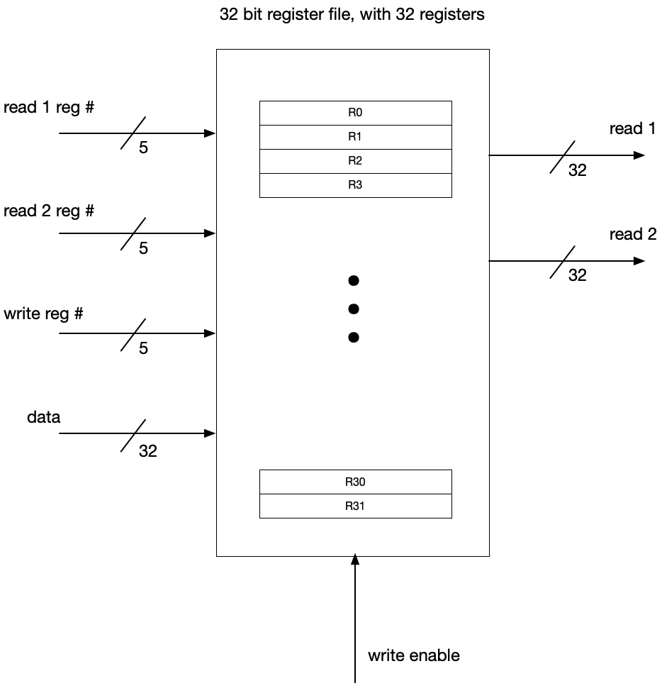
Lines with slashes through them are shorthand for multiple lines, the number of which is indicated next to the slash. So, for example, with 32 registers, we need five bits to specify the register number, hence we have slash 5, on line marked “read 1 reg #.” This input is fed to a decoder to perform line selection.
Decoders
As noted above, decoders are used for register selection within the register file. They’re also used in decoding instructions once fetched.
Multiplexers
Multiplexers (MUXs) are selection circuits. They choose one of a number of inputs and send it to output They are used to choose between different data sources, and within the datapath, are largely controlled by signals from the CPU’s control unit.
In the datapath, MUXes decide:
- which register’s output to use as an operand,
- whether the ALU receives a register or an immediate constant, and
- what the next value of the program Counter (PC) should be.
For example, after a conditional branch instruction, if the condition is false, then program execution proceeds without branching and the value of the program counter is set to the previous value plus four (assuming fixed width, 32-bit instructions). However, if the condition is true, the program counter receives a value corresponding to the branch target (conditional clause, start of loop, etc.) A MUX selects between these two options based on the branch outcome.
This is just one example, MUXs have many other applications, and they appear elsewhere in the datapath.
The program counter (PC)
The Program Counter (PC) is a special-purpose register, which holds the address of the next instruction to execute. Typically, it’s incremented at each cycle by the width of an instruction. Sometimes, it’s updated with a different value based on branch or jump instructions.
For example, without branching, let’s say the program counter held a value value ... 1101 1110 1011 1000, then without branching and assuming fixed-width 32-bit instructions, the next instruction address would end with ... 1101 1110 1011 1100 (incremented by four). Notice that because we’re always incrementing by four, and we want our instructions aligned in memory, the two lowest-order bits are always zero.
Things work differently when branching. Sometimes the program counter is not incremented, but is rather replaced with a new address, the branch target. For example, consider this generic assembly:
MOV  R0, #42      # put constant 42 in R0
MOV  R1, #42      # put constant 42 in R1
CMP  R0, R1       # compare R0 and R1
BEQ  target       # BEQ is "branch if equal"; R0 == R1, so we branch to target
MOV  R2, #0       # we skip this line and go straight to target
target:
MOV  R2, #1       # next instruction to be executed
...
Memory
The datapath accesses memory in two stages:
- instruction memory during the fetch stage, and
- data memory during LOAD or STORE operations.
Memory is external to the CPU core but tightly integrated with the datapath via:
- a read / write interface
- address lines (to specify location), and
- data lines (to send and receive data).
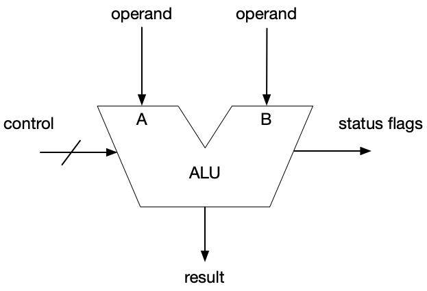
The ALU
The arithmetic logic unit (ALU) performs:
- integer arithmetic (ADD, SUB),
- bitwise operations (AND, OR, NOT, XOR), and
- comparisons (equal to, greater than, less than)
The ALU receives its operands from the register file, performs the computation, and returns the result to either:
- a register (for most operations),
- memory (for STORE instructions), or
- the program counter (for branches).
We’ve only seen a ripple-carry adder, equipped for subtraction, but the ALU includes circuits for bitwise operations and comparisons (the logic unit), a shifter / rotator for bitshift operations, multiplication or division by powers of two, bit field extraction, and other operations.
Example: An ADD instruction adds values in two registers and stores the result in a register. So, ADD R1, R2, R3 tells the CPU to add the values in R2 and R3, and to put the result in R1, that is, R1 = R2 + R3. R2 and R3 are fetched from the register file. They are routed into the ALU, summed, and the result is written to R1.
The ALU includes multiplexers to select operations, operand registers, a result register, and a status flag register which holds condition codes.
When drawing block diagrams, the ALU has a distinctive, notched wedge shape.
The control unit and control signals
While the datapath executes operations, the control unit determines how this is done. The control unit (CU) is the part of the CPU that directs the operation of the processor. It interprets the instruction currently in the instruction register and generates the control signals needed to move data through the datapath, activate functional units, and coordinate memory and I/O operations.
The control unit:
- decodes the instruction fields (op class, opcode, register numbers),
- activates the correct datapath paths using control signals,
- enables the correct write and read paths, and
- ensures correct sequencing and operation.
There are two main implementation styles:
Hardwired control
A hardwired control unit uses fixed logic circuits—gates, decoders, and flip-flops—to generate control signals directly from the instruction bits and timing signals.
Advantages:
- Very fast, since control signals are produced by combinational logic.
- Efficient for simple, regular instruction sets (e.g., RISC architectures).
Disadvantages:
- Inflexible—modifying the instruction set or adding new instructions requires redesigning and fabricating new hardware.
- Difficult to debug or extend once implemented.
Example: Most modern RISC processors (including ARM) use hardwired control for speed.
Microprogrammed control
A microprogrammed control unit stores the control logic in memory—in the form of microinstructions within a control store. Each microinstruction defines a pattern of control signals for one step of instruction execution. A microsequencer reads these microinstructions in sequence to orchestrate the datapath.
Advantages:
- Flexible and easy to modify—new instructions or addressing modes can be implemented by changing the microcode.
- Simplifies design for complex instruction sets (CISC).
Disadvantages:
- Slower, since each machine instruction may require fetching and interpreting multiple microinstructions.
- Consumes more memory for the control store.
Example: Classic CISC processors like the Intel 8086 and VAX used microprogrammed control.
© 2025 Clayton Cafiero.
No generative AI was used in writing this material. This was written the old-fashioned way.