Transistor logic

Recall that a transistor is an electrically-controlled switch. Let’s explore that in a little more detail.
We’ll look at simplified views of transistors which are at the heart of all logic and computation in a computer. These are metal-oxide semiconductor transistors, abbreviated MOS. There are two types, NMOS and PMOS—N-type metal-oxide semiconductor and P-type metal-oxide semiconductor. We don’t need to concern ourselves with how they are made, or the materials used, or the physics of how they work. We can just focus on how they behave in small circuits.
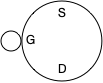
Here’s how we’ll draw these two types of transistor. First, an NMOS.

Here’s how an NMOS transistor works. If there is a source of current connected to terminal S (source), and there’s a low voltage at the gate (G), current will not flow between source and drain (D). However, if sufficient voltage is applied to the gate, current will flow from source to drain.
It’s just an electrically-controlled switch. Apply voltage to the gate, and it opens, letting current flow. Turn off the voltage to the gate, and it switches off.
Now for the PMOS variety.
Here’s how a PMOS transistor works. If there is a source of current connected to terminal S (source), then if a low voltage is present at the gate (G), current will flow between source and drain (D). However, if sufficient voltage is applied to the gate, current will not flow from source to drain.
Again, it’s just an electrically-controlled switch, but one that’s complementary to the NMOS type. Apply voltage to the gate, and it closes, and no current flows. Turn off the voltage to the gate, and it opens, letting current flow.
You can see that these two types are complementary. Circuits constructed with these two types are called CMOS circuits (CMOS = complementary metal-oxide semiconductor).
Now let’s look at a circuit constructed from two of these devices—one of each.
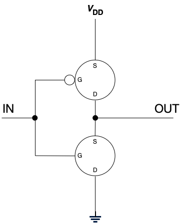
In this diagram, you’ll see some additional elements.

You may think of V_{DD} and the symbol to the right of it as a source for current and a drain or destination for current, respectively. The black dot indicates a junction where wires are connected. If wires cross and there is no black dot (junction) then the wires are not connected.
Before you read on, ask yourself what this circuit does. What is the output (at OUT) if the voltage at IN is high? What is the output (at OUT) if the voltage at IN is low?
This circuit is what we call an inverter. If we have a 1 (voltage present) at the input, the output is 0. If we have a 0 (no voltage present) at the input, the output is 1.
(For the astute reader: Yes, you can construct an inverter from a single PMOS transistor. However, we construct inverters using this two transistor design because this design reduces power consumption, produces strongly differentiated outputs, can switch more quickly, and is more robust to noise.)
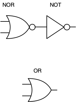
An inverter is a common component so it has its own symbol.
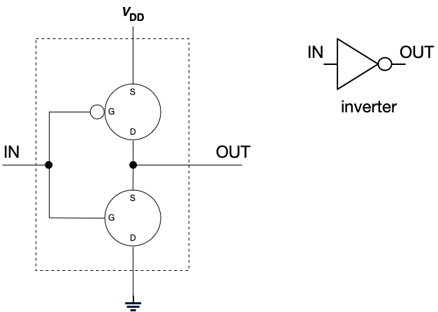
Consider the truth table for an inverter. It’s exactly the truth table for negation! Accordingly, we often call this a NOT gate.
| P | \neg P |
|---|---|
| 0 | 1 |
| 1 | 0 |
| IN | OUT |
|---|---|
| 0 | 1 |
| 1 | 0 |
Imagine that.
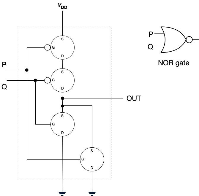
Now we’ll make another, this time with four transistors.
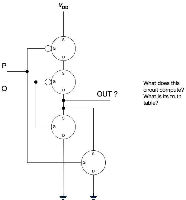
Again, before you read on, ask yourself what logical operation this circuit performs. Construct a truth table:
| P | Q | OUT |
|---|---|---|
| 0 | 0 | |
| 0 | 1 | |
| 1 | 0 | |
| 1 | 1 |
This circuit computes NOT OR, shortened to NOR.
| P | Q | NOR |
|---|---|---|
| 0 | 0 | 1 |
| 0 | 1 | 0 |
| 1 | 0 | 0 |
| 1 | 1 | 0 |
Again, because it’s commonly used, this one has its own symbol too.
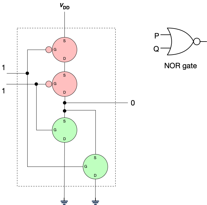
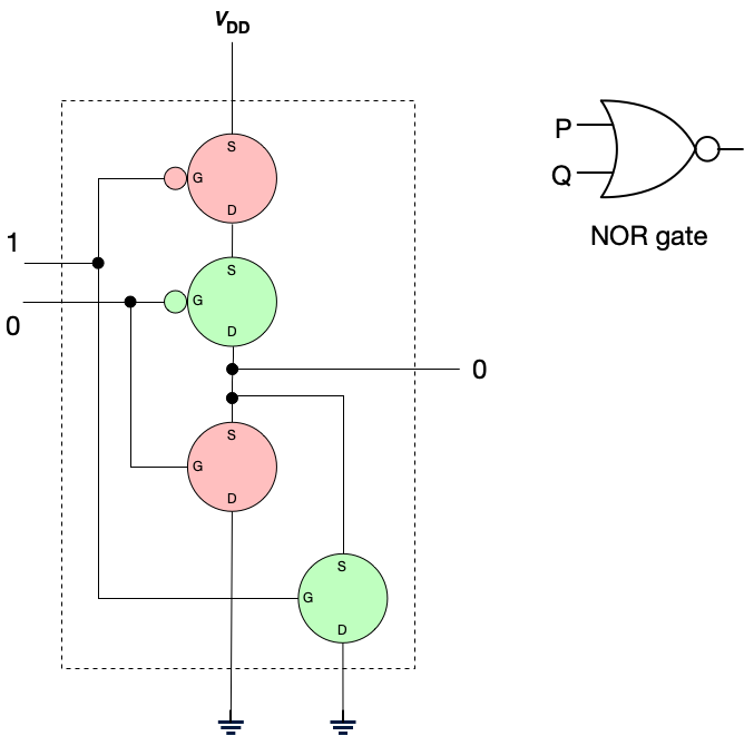
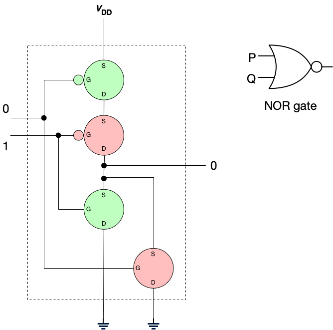
Let’s see how this works. I’ll color transistors permitting flow green, and those that do not permit flow rose. Hopefully this will make the operation of this gate clear. We’ll examine all possible inputs (from the truth table) and examine the outputs.
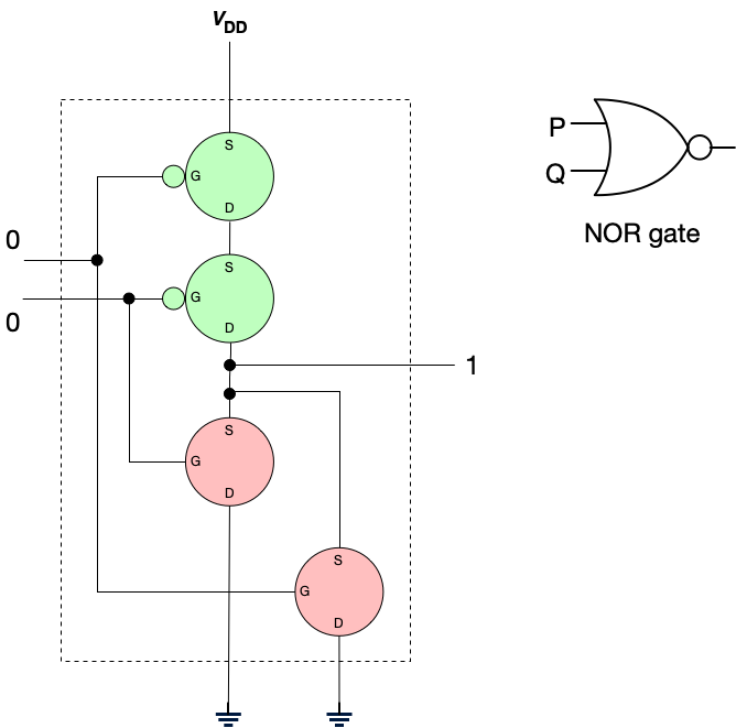
The NOR gate is often called a “universal gate” because it can (in principle) be used as a component to construct gates to perform any other logical operation.
Let’s not go that route, and instead see how we can construct an OR gate using a NOR and a NOT.
All we need to do is connect a NOT gate (inverter) to the output of a NOR gate, and we get an OR gate. Think of double-negation elimination, if NOR is NOT OR, then by inverting the output we get NOT NOT OR, and the two NOTs cancel, leaving OR.
Exercises
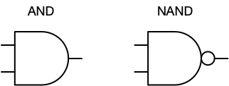
Using only NOR gates, construct a circuit that computes AND. Hint: You can do this with three NOR gates.
Using only NOR gates, construct a circuit that computes NAND. Hint: You’ll need four NOR gates for this.
If you’ve completed a NOR gate, produce a different construction for an AND gate. Hint: You can do this with two NAND gates.
© 2025 Clayton Cafiero.
No generative AI was used in writing this material. This was written the old-fashioned way.