Latch and flip flop
Here we’ll learn about important sequential circuits that are used in many applications including memory, registers, and flags.
A sequential circuit is one whose output depends not only on its current input(s) but also on past inputs. Perhaps the most important application of a sequential circuit is to maintain state.
Memory and registers are examples of circuits that maintain state—they “remember” stored values. This is what we mean by “maintaining state.”
Two important circuits we can construct from logic gates are latches and flip-flops. Here we will look at three types: SR latches, D latches, and D flip-flops.
SR latch
An SR latch is a circuit that can store one bit of information. “SR” is an abbreviation of set-reset. An SR latch can be constructed using two NOR gates.
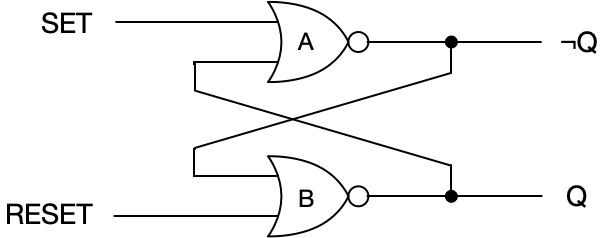
The purpose of this circuit is, as stated, to store one bit of information. Notice that the inputs are labeled “SET” and “RESET”, this indicates their function.
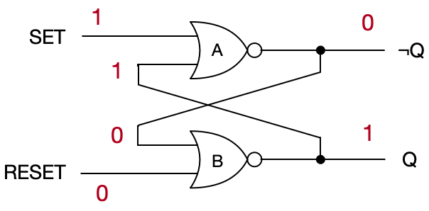
- A SET input, \text{SET} = 1, \text{RESET} = 0, is used to force the latch to produce Q = 1 and \neg Q = 0.
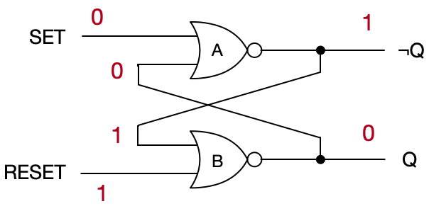
- A RESET input, \text{SET} = 0, \text{RESET} = 1, is used to force the latch to produce Q = 0 and \neg Q = 1.
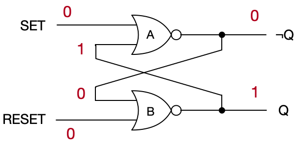
- Input of \text{SET} = 0, \text{RESET} = 0 does not change the current state.
- Input of \text{SET} = 1, \text{RESET} = 1 is prohibited and prevented by circuitry upstream from the latch.
Let’s think about what goes on with this circuit. Notice that we take the output of each of the NOR gates and use these as input to the other NOR gate—there are feedback loops built into this circuit.
Recall that a NOR gate will produce 1 if and only if both inputs are 0.
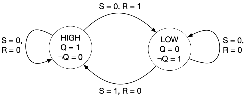
The SR latch is what we call bistable—it has two stable states.
- HIGH: Q = 1 and \neg Q = 0, or
- LOW: Q = 0 and \neg Q = 1.
When first powered up, the cross-coupled NOR gates do not have “guaranteed” output. Due to tiny imbalances, noise, or other factors, left alone this circuit will settle into an indeterminate state. This, of course, is no good for a digital computer so additional circuitry and signals are used to force an SR latch into one of its two bistable states (e.g. a RESET signal to force the latch to LOW or a PRESET signal to force the latch to HIGH).
Let’s assume that the latch has received a RESET signal, and it is currently in the LOW state. As as long as power is applied to this circuit, it’ll be stable (unless new signals are received).
Now say, we sent a 1 on the \text{SET} wire, and a 0 on the \text{RESET} wire—that’s a SET signal. Because of the latch’s previous state LOW, NOR gate A gets (1, 0) and emits a 0. NOR gate B gets (0, 1) and it too emits a 0. But remember, we still have the SET signal present. Feedback continues and A gets (0, 0) and emits a 1, B gets (1, 1) and emits a 0. Now A continues to get (0, 0) and continues to emit 1, and B continues to get (1, 1) and continues to emit a 0. The circuit has reached a stable state: HIGH.
Now let’s see what happens if we apply a NO CHANGE signal, that’s a 0 on the \text{SET} wire, and a 0 on the \text{RESET} wire. The latch’s previous state was HIGH, so gate A gets (0, 0) and emits 1. Gate B gets (0, 1) and emits 0. The state of the latch does not change! It remains stable, in the HIGH state.
Now let’s send a RESET signal, that’s a 0 on the \text{SET} wire, and a 1 on the \text{RESET} wire. The latch was in the HIGH state, so gate A gets (1, 1) and emits a 0, and gate B gets (0, 0) and emits 1. The circuit is now stable in the LOW state.
We can draw a state diagram for our SR latch, which indicates its behavior at a somewhat higher level of abstraction.
Solving equations for an SR latch
Tracing the feedback loop in a latch is troublesome, error-prone (at least with pencil and paper) and perhaps not the best approach to figuring out the behavior of a latch. Fortunately, there’s another way.
First, let’s introduce a little new notation. We write Q' (pronounced “Q prime”) to mean the complementary output provided by the circuit. It is our objective, in fact a design intention, that Q' \equiv \neg Q. But until the circuit has reached a stable state this is not always the case—it takes some time for feedback to propagate and to arrive at a stable state. During switching, delays in propagation can result in (very, very briefly) Q' \neq \neg Q.
We use Q' in solving equations to determine the new state of a latch upon receiving new input. For example, for an SR latch with cross-coupled NOR gates, we have
\begin{align*} Q &= \neg(R \lor Q')\\ Q' &= \neg(S \lor Q) \end{align*}
So given a SET signal (S = 1, R = 0), we have
Q' = \neg(S \lor Q) = \neg(1) = 0,
and
Q = \neg (0 \lor 0) = \neg(0) = 1.
So on a SET signal, we get Q' = 0, Q = 1, and the stable state \neg Q = 0, Q = 1.
Let’s see what happens with a RESET signal (S = 0, R = 1). Again,
\begin{align*} Q &= \neg(R \lor Q')\\ Q' &= \neg(S \lor Q) \end{align*}
Plug and chug:
Q = \neg (1 \lor Q') = \neg(1) = 0,
and
Q' = \neg(0 \lor Q) = \neg(0) = 1.
So on a RESET signal, we get Q' = 1, Q = 0, and the stable state \neg Q = 1, Q = 0.
On a NO CHANGE signal (R = 0, S = 0), again
\begin{align*} Q &= \neg(R \lor Q')\\ Q' &= \neg(S \lor Q) \end{align*}
which reduces to
\begin{align*} Q &= \neg(Q')\\ Q' &= \neg(Q) \end{align*}
and we have two stable solutions Q = 0, Q' = 1 or Q = 1, Q' = 0, and the latch just “remembers” its previous state.
Remember that the input, S = 1, R = 1 is prohibited.
A “next state” table
It’s common to produce a “next state” table for a latch (or flip-flop) which shows the result we reach given a current state and some input. Since Q and \neg Q are complementary when stable, we just ignore \neg Q in the table, with the understanding that it’s always the complement of Q, whatever Q is.
| S | R | Q | Q_{\text{NEXT}} | comment |
|---|---|---|---|---|
| 0 | 0 | 0 | 0 | NO CHANGE |
| 0 | 0 | 1 | 1 | NO CHANGE |
| 1 | 0 | 0 | 1 | SET |
| 1 | 0 | 1 | 1 | SET |
| 0 | 1 | 0 | 0 | RESET |
| 0 | 1 | 1 | 0 | RESET |
| 1 | 1 | n/a | n/a | forbidden |
| 1 | 1 | n/a | n/a | forbidden |
The SR latch: summary
An SR latch is bistable, with two stable states that we label LOW and HIGH. In a cross-coupled NOR construction, these correspond to Q = 0 and \neg Q = 1, and Q = 1 and \neg Q = 0, respectively. A SET signal forces the latch into a stable, HIGH state. A RESET signal forces the latch into a stable, LOW state. A NO CHANGE signal does nothing, and the latch remains in whatever state it was in. An input of 1 on the \text{SET} wire and a 1 on the \text{RESET} wire is prohibited by upstream circuits. It works similarly for the cross-coupled NAND construction, with signals and states inverted.
Because it can be set and reset easily, and because it can maintain state, an SR latch remembers its state until it’s told to change it!
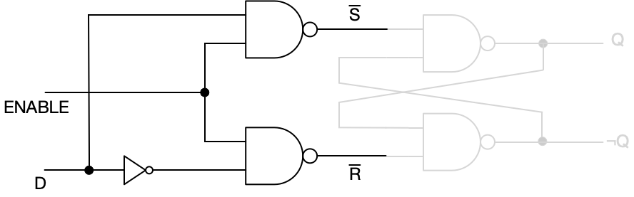
D latch
As mentioned, an SR latch requires additional upstream circuitry to prevent receiving a prohibited signal which would leave it in an unstable state.
Here’s another latch design with precisely that kind of upstream circuitry: a D latch.
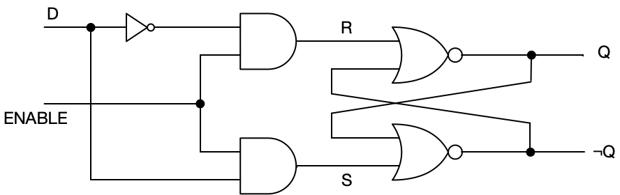
As with the SR latch, there are two constructions, one with cross-coupled NOR gates, the other with cross-coupled NANDs.
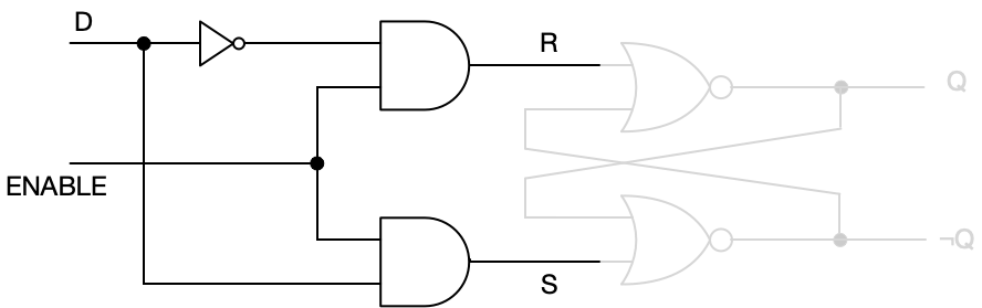
Let’s look at the upstream circuitry in the cross-coupled NOR construction in isolation for a moment. This consists of two AND gates and an inverter.
Here’s a truth table for this portion of the circuit.
| ENABLE | D | S | R | signal |
|---|---|---|---|---|
| 0 | 0 | 0 | 0 | NO CHANGE |
| 0 | 1 | 0 | 0 | NO CHANGE |
| 1 | 0 | 0 | 1 | RESET |
| 1 | 1 | 1 | 0 | SET |
For this circuit, all the outputs correspond to one of the permitted input signals to a cross-coupled NOR SR latch: (S=0, R=0) is NO CHANGE, (S=0, R=1) is RESET, and (S=1, R=0) is SET. There are no other possible outputs from this circuit—there’s no combination of inputs that gives us the prohibited (S=1, R=1). The prohibition is enforced! Notice also that if enabled, the output signal is entirely determined by the input on the D line. If there’s a 1 on the D line, the output is a SET signal; if it’s a 0, then the output is a RESET signal.
So when we hook this up to an SR latch, we have a circuit that guards against prohibited inputs, and SET / RESET behavior is driven by the data (D) line.
Here’s a complete truth table (where Q_{\text{NEXT}} is the value of Q after receiving the signal.
| ENABLE | D | S | R | signal | Q | Q_{\text{NEXT}} |
|---|---|---|---|---|---|---|
| 0 | 0 | 0 | 0 | NO CHANGE | 0 | 0 |
| 0 | 0 | 0 | 0 | NO CHANGE | 1 | 1 |
| 0 | 1 | 0 | 0 | NO CHANGE | 0 | 0 |
| 0 | 1 | 0 | 0 | NO CHANGE | 1 | 1 |
| 1 | 0 | 0 | 1 | RESET | 0 | 0 |
| 1 | 0 | 0 | 1 | RESET | 1 | 0 |
| 1 | 1 | 1 | 0 | SET | 0 | 1 |
| 1 | 1 | 1 | 0 | SET | 1 | 1 |
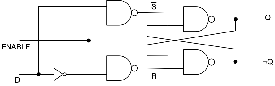
It works similarly for a cross-coupled NAND construction. The upstream portion of this circuit consists of two NAND gates and an inverter.
Here’s a truth table for this portion of the circuit.
| ENABLE | D | \overline{S} | \overline{R} | signal |
|---|---|---|---|---|
| 0 | 0 | 1 | 1 | NO CHANGE |
| 0 | 1 | 1 | 1 | NO CHANGE |
| 1 | 0 | 1 | 0 | RESET |
| 1 | 1 | 0 | 1 | SET |
Remember that a cross-coupled NAND SR latch is active low, so the signals are different. All the outputs correspond to one of the permitted input signals to a cross-coupled NAND SR latch: (\overline{S}=1, \overline{R}=1) is NO CHANGE, (\overline{S}=0, \overline{R}=1) is SET, and (\overline{S}=1, \overline{R}=0) is RESET. There are no other possible outputs from this circuit—there’s no combination of inputs that gives us the prohibited (\overline{S}=0, \overline{R}=0). The prohibition is enforced! Notice also that if enabled, the output signal is entirely determined by the input on the D line. If there’s a 1 on the D line, the output is a SET signal; if it’s a 0, then the output is a RESET signal.
So, again, when we hook this up to an SR latch, we have a circuit that guards against prohibited inputs, and SET / RESET behavior is driven by the data (D) line.
Here’s a complete truth table for the cross-coupled NAND construction (where Q_{\text{NEXT}} is the value of Q after receiving the signal.
| ENABLE | D | \overline{S} | \overline{R} | signal | Q | Q_{\text{NEXT}} |
|---|---|---|---|---|---|---|
| 0 | 0 | 1 | 1 | NO CHANGE | 0 | 0 |
| 0 | 0 | 1 | 1 | NO CHANGE | 1 | 1 |
| 0 | 1 | 1 | 1 | NO CHANGE | 0 | 0 |
| 0 | 1 | 1 | 1 | NO CHANGE | 1 | 1 |
| 1 | 0 | 1 | 0 | RESET | 0 | 0 |
| 1 | 0 | 1 | 0 | RESET | 1 | 0 |
| 1 | 1 | 0 | 1 | SET | 0 | 1 |
| 1 | 1 | 0 | 1 | SET | 1 | 1 |
The D latch: summary
Like an SR latch, a D latch is bistable, with two stable states that we label LOW and HIGH. In a cross-coupled NOR construction these correspond to Q = 0 and \neg Q = 1, and Q = 1 and \neg Q = 0, respectively. However, SET and RESET signals are conditioned on upstream circuitry. If the circuit is enabled, then whatever arrives on the data line determines the output, and we sometimes say the circuit is transparent. If the circuit is not enabled, then it maintains state, and whatever appears on the data line is ignored. It works similarly for a cross-coupled NAND construction with internal SET, RESET signals inverted, and low-active states.
Flip-flops
As fast as signal propagation is in modern semiconductor circuits, it is not instantaneous. Every gate we add in a signal path increases propagation time. Moreover, even with on-chip CMOS logic, change of state in a latch takes somewhere between hundreds of picoseconds to a few nanoseconds to settle in to a new bistable state. Because signals have different propagation times (depending on the size and type of circuit) this would create difficulties if there were no way of synchronizing circuits. If you think of the fetch-decode-execute cycle, for example, chaos would rule the day if everything didn’t proceed in lockstep.
Clock signals are precisely timed pulses of zeros and ones.
Consider what would occur if we connected a clock to the ENABLE input of a D latch. A D latch is transparent while the clock (or enable) signal is active. That means when the clock = 1 (for a positive-level latch), any change at D immediately propagates to Q. When the clock = 0, the latch “closes” and holds the last value.
That’s fine in isolation, but it causes a problem in synchronous circuits: if a latch feeds into logic that drives another latch controlled by the same clock, data can race through both latches during the same clock pulse—a race or transparency problem.
Accordingly, much of what goes on in a computer is synchronized to a clock (in fact, different subsystems or components may have their own clocks, but we’ll ignore that for now).
One example of a synchronous sequential circuit is the flip-flop. A flip-flop stores one bit of information, and it is synchronized with a clock. Its state can only change upon a trigger from a clock, typically the rising edge of a clock pulse.
The most common flip-flop is the D flip-flop. A D flip-flop has two inputs: D (data) and C (clock). On the rising edge of the clock, the value on D is stored and appears on the output Q (and the complementary output on \neg Q). Until the next trigger, the output remains constant, regardless of changes to D. This makes flip-flops predictable and reliable building blocks for synchronized sequential circuits. Use of these and other synchronized circuits ensures that data flows through the system in an orderly fashion.
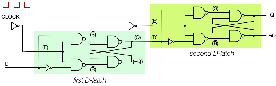
You see from the diagram above that a D flip-flop is constructed from two latches, and that their clock inputs are inverted with respect to one another. That gives us two latches that are sensitive to opposite clock phases.
| clock phase | first latch | second latch |
|---|---|---|
| 0 (LOW) | enabled / transparent | disabled / closed |
| 1 (HIGH) | disabled / closed | enabled / transparent |
The two-latch pair is the foundation of an edge-triggered D flip-flop. During the clock’s LOW phase, the first latch reads from the data line, D, and this propagates to its output. During the clock’s HIGH phase, the second latch reads the value stored in the first, and the first ignores new changes. Because one latch is open when the other is closed and vice versa, this is called a “flip-flop.” The result is that the output only changes once per clock cycle, right at the clock transition—giving edge-triggered behavior.
You can think of the two-latch arrangement as a buffered pipeline. The first latch captures the input while the clock is low. The second latch emits that captured value when the clock rises. Because they’re never open at the same time, the signal can’t race through both—the signal moves one stage per clock edge. We need two latches so that the circuit responds only to the transition of the clock rather than its level. That’s what turns a level-sensitive latch into an edge-triggered flip-flop.
Flip-flop summary
A flip-flop is a synchronous sequential circuit that stores one bit of information, and any state changes are synchronized to a clock.
Summary: latches and flip-flops
The SR latch stores, the D latch controls when to store, and the D flip-flop synchronizes storage with a clock.
© 2025 Clayton Cafiero.
No generative AI was used in writing this material. This was written the old-fashioned way. However, generative AI may have been used in proofreading certain passages for accuracy to supplement review by human proofreaders with domain knowledge.