Chip fabrication

Please see: Section 1.5 in textbook: Technologies for Building Processors and Memory, pp. 24–28.
- Transistor: “A transistor is simply an on/off switch controlled by electricity.”
- Integrated circuit: “[Combining] dozens to hundreds of transistors into a single chip.”
- VLSI: Very large-scale integrated circuit (think millions to billions of transistors)
Basic manufacturing
Wafers are made of silicon and other materials, e.g., gallium nitride, gallium arsenide. Wafers are polished to be extremely smooth (if we’re going to build on a nanometer scale, we can’t have imperfections).
Materials are deposited on the wafer in very thin layers (again, at a nanometer scale). Deposition is usually done with vapor—that’s how thin these layers are. Then a light-sensitive coating called a “photoresist” is applied, and then the wafer is etched by exposure to deep UV light or extreme UV light. When the photoresist is developed there’s a pattern that protects (insulates) certain areas and exposes others. Exposed regions are “doped” with impurities (boron, phosphorous, arsenic, etc.) to give these areas the desired properties so they can function as transistors. This cycle of deposition and etching takes place many times to build up multiple layers of components on the wafer. Sometimes the wafer is polished in between steps (called “planarization”).
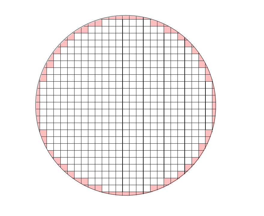
When this process is complete, the wafer holds many identical dies and is ready to be cut. Because the wafer is round, and the dies are square, there’s some loss around the edge.
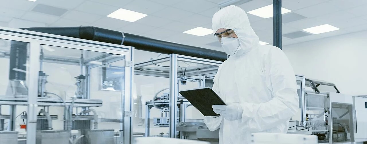
Once cut into individual dies, the dies are packaged (with all connectors installed), and tested. Because even the smallest imperfect can make a die unusable, this all takes place in a ultra-clean environment.
© 2025 Clayton Cafiero.
No generative AI was used in writing this material. This was written the old-fashioned way.